Design and application of metamaterials

Motivation
Electromagnetic metamaterials (EM) are synthetic structures with special electromagnetic properties such as negative value of the refractive index – as postulated by Veselago. They have become an active research area because they exhibit unusual EM responses not attainable with natural materials. Some attractive application examples are in superlensing, cloaking, artificial magnetic conductance and more generally, coordinate transformation material design. As a one way to realize such functionalities, periodic or semi-periodic arrays of resonant structures such as split-ring resonators (SRRs) have been used. Second way to realize such functionalities, full 3D dielectric structure based on period 3D unit cell have been used.
To realize modeling of these structures, (distributed) circuit model-based and full EM-simulation model based have benn used.
- Research directions
In case of metasurface (fig 1. A) most interesting phenomena are associated with a network of resonators (SRR). Based on this fact modeling of this structures takes account model of single SRR, and model of couplings in rezonator network. These models can be based on full Electromagnetic field simulation and (distributed) circuit model.
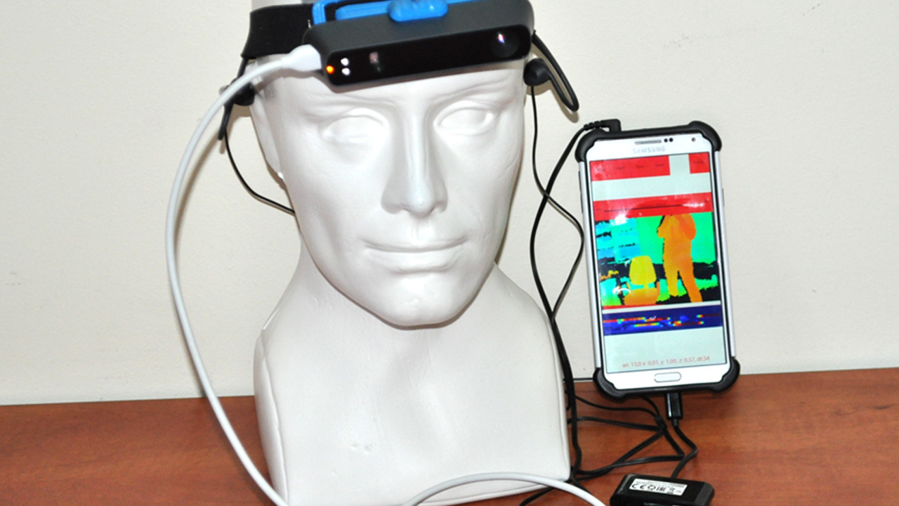
This is a first direction of research: method for effective modeling of metasurface. Further research directions are connected with metamaterials applications: for medical diagnostic (e.g. MRI lens), telecommunication (Artifical Magnetic Conductor - AMC, Electromagnetic Band Gap EBG and other) and biosensors in THz gap.
Dielectric 3D metastructures are a separate research direction. In this case, the key issues are: application of transformation optics methods for numerical EM field shaping, generating periodic 3D structures, full Electromagnetic field simulation and preparing 3D models (by 3D printer).
In fact, research are included: circuit theory, description of the behavior of the electromagnetic field in various materials, EM full field simulation, transformation optics, optimization methods, 3D printing problems and others.

Fig 1: Examples of metamaterials: (A) mu-negative metasurfaces, (B) full 3D dielectric metamaterials.
- Achievements
At the Institute of Electronics, we conduct research on modeling the metasurfaces for : magnetic resonance imaging (magnetic lens), Artifical Magnetic Conductors - AMC and Electromagnetic Band Gap EBG for telecommunication application, for example in BAN network (Body Area Network), finally also for metasurfaces designed for THz Gap.
- Perspectives
At present, our priority is that the acquired competencies in building and applying metasurfaces for given applications (medical, telecommunication and others).
- Contact persons
- Prof. Sławomir Hausman
 , e-mail: This email address is being protected from spambots. You need JavaScript enabled to view it.
- Dr. Łukasz Jopek, e-mail: This email address is being protected from spambots. You need JavaScript enabled to view it.
- Prof. Sławomir Hausman
- Relevant publications